
|
|
|
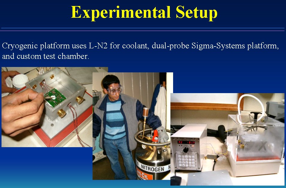
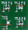
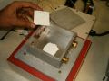
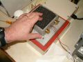
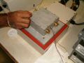
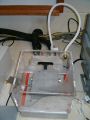
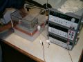
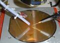
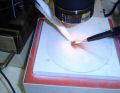
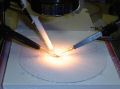
While both considerations are being studied throughout the project, work at K-State has concentrated mainly on the first. Circuits are tested in a custom cryogenic facility shown here. Reliability studies of electronics at these temperartures are being carried out by JPL under separate projects .
Parametric Drift in Analog/RF Circuits
Test Setup for COTs TCXO and Filter Measurements
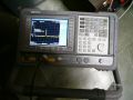
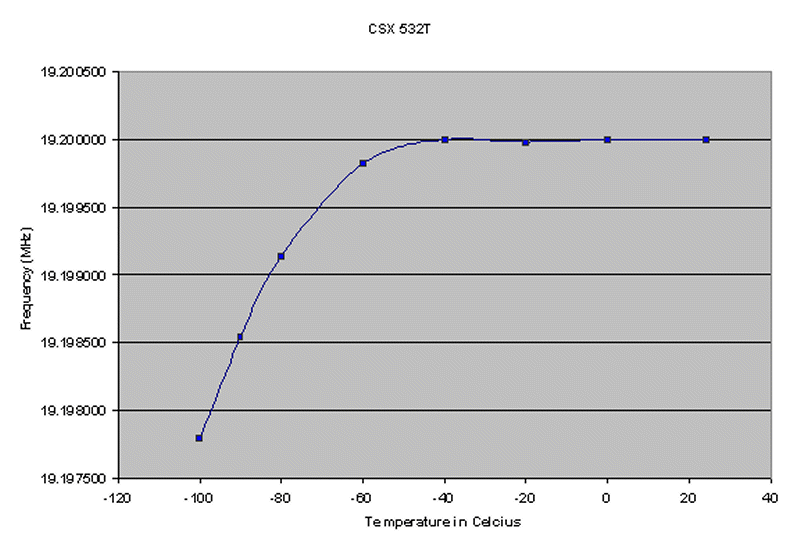
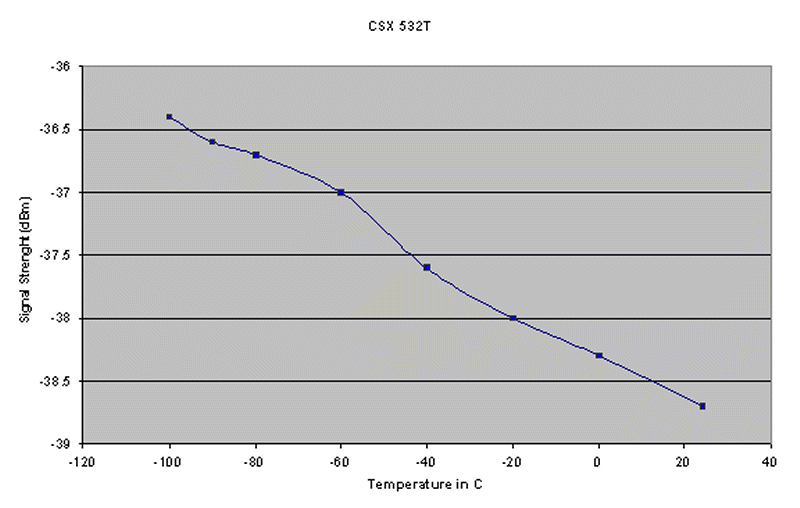
Representative TCXO Measurement Results
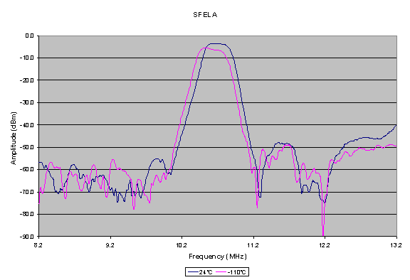
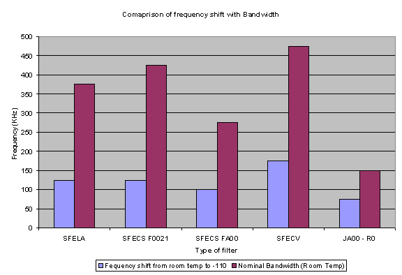
Representative IF Filter Measurement Results
Test Setup for PCM Wafer-level Measurements
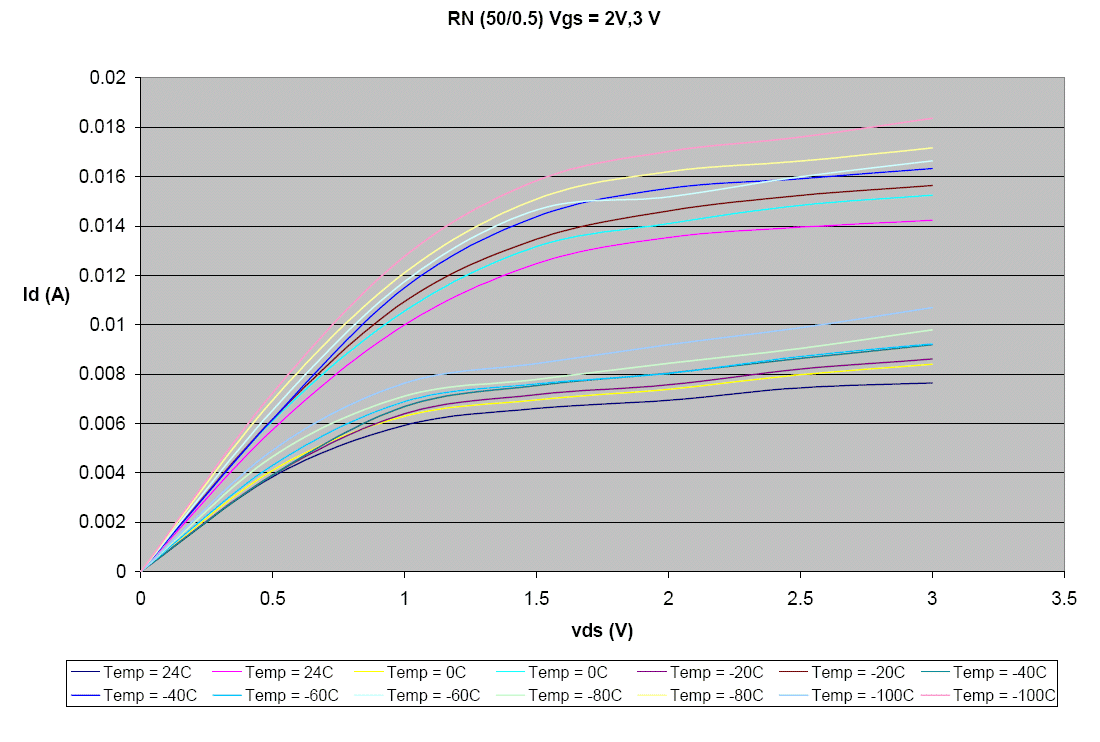
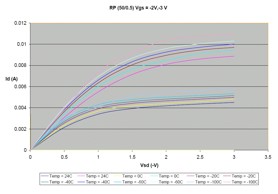
Example Transistor Measurement Results
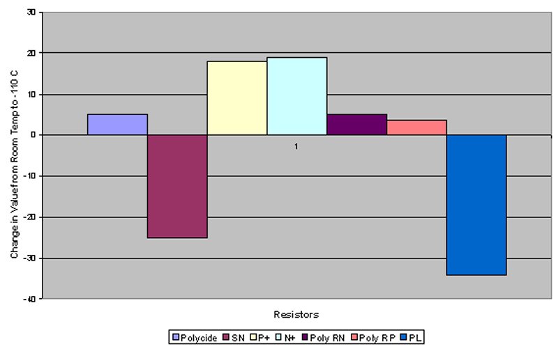
Summary of Resistor Measurement Results
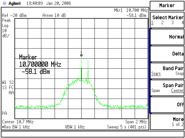
Conclusions While the filters and TCXO devices both show substantial shifts in frequency below -40 C, both shift downward by an acceptable amount. Using a nominal 300 kHz IF bandwidth, the shifts are less than 1/2 of the bandwidth so that the signal stays within the filter passband. Moreover, the profile for each is similar, so that to a first order, the signal can be kept centered in the passband by using high-side injection in the receiver architecture. Shifts in the parameters of the active and passive devices match the existing Peregrine toolkit models reasonably well, even though the models were not developed at low temperature. For cases where critical values must be determined, the measured data elaborated in Yogesh Tugnawat's thesis can be used. In addition, it is possible to build temperature compensation in biasing and amplifier circuits thanks to the existence of resistors with both positive and negative coefficients. This strategy has been successfully applied in the high-gain IF circuits of the microtransceiver with measured gain shifts of less than 3 dB from +25 to -100 C. The combined use of high-side injection at the architecture level and careful temperature compensation in the circuit design is illustrated in the annimated graphic below. Here, the output of the IF filter is shown for the case of a -100 dBm RF input signal at 435.7 MHz with the synthesizer tuned to 446.4 MHz As expected, the signal stays well-centered in the passband and the overall conversion gain is nearly constant. Note also the decrease in noise floor as the temperature is lowered, as expected. (These results are from the first RFIC prototype which has some spurious responses due to harmonics of the internal divide-reference frequency, seen in figure at 100 kHz offset, and higher than targeted overall system noise figure due to insufficient LNA gain. Both problems have been corrected in the fab-2 circuits currently undergoing test.
Back to Microtransceiver main page...
|