
|
|
|
Designing for the Martian Environment The ultimate goal of this project is to develop a transceiver prototype at Technology Readiness Level 5 - suitable for operation in the Martian Environment. This is being achieved through robust design practices including low-risk transceiver architectures, up-front assessment of component performance at cryogenic temperatures, selection of a space-proven radiation-hard IC process, and iterative design of RFIC chips to refine and optimize performance In addition, extensive testing is used throughout the project. This page shows some of the testing activities to-date (through July 2007) including:
Early Demonstration Board Early "Fab 0" prototypes of RFIC transmitter circuits and digital bit encoding circuits have been assembled into a demonstration PC board and tested from 1 kbps to 1024 Mbps. Photos below show the PC board together with spectrum and constellation plots for BPSK and RC-BPSK modes as well as an unmodulated carrier. Although this prototype does not include an RF power amplifier and is therefore limited to about 0dBm output, the tests provided important information used in later RFIC designs.
This demo board has been successfully paired with a Satcom receiver to demonstrate live, over-the-air transmissions.
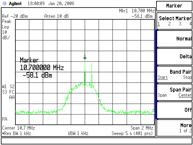
Fab1: First Receiver RFIC Prototype The first receiver circuit RFIC was completed in 2005. Testing took place in two stages, starting with chip-level measurements of circuit blocks such as the LNA and IF amplifiers, and then proceeding to a full PCB test. Measurements are used to verify operation and to refine subcircuit performance in subsequent fabrication runs. These photos and figures show example measurements of the LNA at the chip level from fab 1 measurements.
Following chip-level tests, the IC is incorporated into a PC board for overall functional, performance, and temperature testing. Photos below show the PC board together with the spectrum of the 1-bit IF ADC output sampled at 19.2 MHz.
Temperatue testing was then done to assess the operation of the receiver prototype IC at temperatures from +25C (room temperature) down to -110 C (the limit of the test setup). The animated GIF below illustrates the signal at the output of the if filter using a -100 dBm unmodulated carrier. The IF signal remains centered within the passband throughout the temperature range and drifts downward in frequency by the predicted amount (50 kHz). Moreover, the gain stays constant to better than 3 dB and the noise floor falls predictably due to the cryogenic cooling of the circuits. Please see the Cryogenic Electronics page for additional information. Note that these results are from the first RFIC prototype which has some spurious responses due to harmonics of the internal divide-reference frequency, seen in figure at 100 kHz offset, and higher than targeted overall system noise figure due to insufficient LNA gain. Both problems have been corrected in the Fab-2 RFIC prototype circuits tested in Spring/Summer of 2006.
Fab2: First Transmitter RFIC Prototype The first full transmitter circuit RFIC was completed in early 2006. The chip contains fully-integrated 10 mW and 100 mW power amplifiers in addition to a refined frequency synthesizer providing fractional-N division for fine tuning steps. Also included are a re-spin of the receiver LNA, a mixer to allow assessment of noise from the synthesizer into the LNA/RX circuitry, and various test structures for assessment of individual blocks and components such as spiral inductors. Example test results are illustrated below:
Fab3: 1-Watt Power Amplifier IC The 1-Watt power amplifier needed to provide higher data return rates from the microtransciever was also tested in 2006. Sample photos and measurement data are shown below. Additional details will be provided following publication of results in early 2007:
Fab4: Fully-integrated Transceiver Based on the Fab1 and Fab2 designs, a full transceiver prototype was implemented in the Fab 4 run. All essential functions of the IC have been successfully tested so that this chip can serve as the final prototype for the project. A set of "minor bugs" has been documented and can be used in future development projects required to bring the RFIC to a flight-ready status. Despite these minor bugs, the Fab4 design is fully operational and usable for proof-of-concept TRL-4/5 demonstrations.
To provide full testing of the micro-transceiver, a demonstration board was developed using the Fab 1 receiver RFIC, the Fab 2 transmitter RFIC, and a commerical FPGA for the digital modem circuits. Interfaces include an SMA antenna connector, a JTAG programming connector, and CMOS-level I/O headers for connection to test equipment. Preliminary testing shows that the RFICs and FPGA are functional. The photos below show the board, together with receiver testing using -100 dBm RF inputs. Performance testing using this board is currently on-going and is expected to be completed in the first quarter of 2007. When the Fab 4 Transceiver chip is complete and tested, this demo board will be revised to a single-chip RFIC (plus optional 1W PA chip) design and receiver sensitivity is expected to improve by approximately 10 dB:
Full-Transceiver Evaluation Board Development The final deliverable from this project is an "Evaluation Board" that is used for system-level testing with Mars infrastructure asset engineering models, and for use by Mission Planners considering the microtransceiver for future Scout development work. The board was successfully designed and constructed in mid-2007 and is currently being used to refine the RFIC operation and to test the digital modem code using an on-board Xilinx FPGA. It is expected to be fully operational in late 2007.
Back to Microtransceiver main page...
|